

Semiconductor gamma-ray and X-ray detectors are being used increasingly in medicine, industry, astronomy and national security. Conventional semiconductor detectors are manufactured from germanium and silicon.
Such materials have become less useful in many emerging applications due to their physical limitations such as low detection efficiency or their need to operate at cryogenic temperatures.
This research contributes towards the development of compound semiconductor radiation detectors based on cadmium manganese telluride (CdMnTe) that operate at room temperature and with a high stopping power.
With continued improvements in crystal quality and detector fabrication, this research could lead to the development of a new generation of radiation detectors for use in medical imaging and in national security applications.
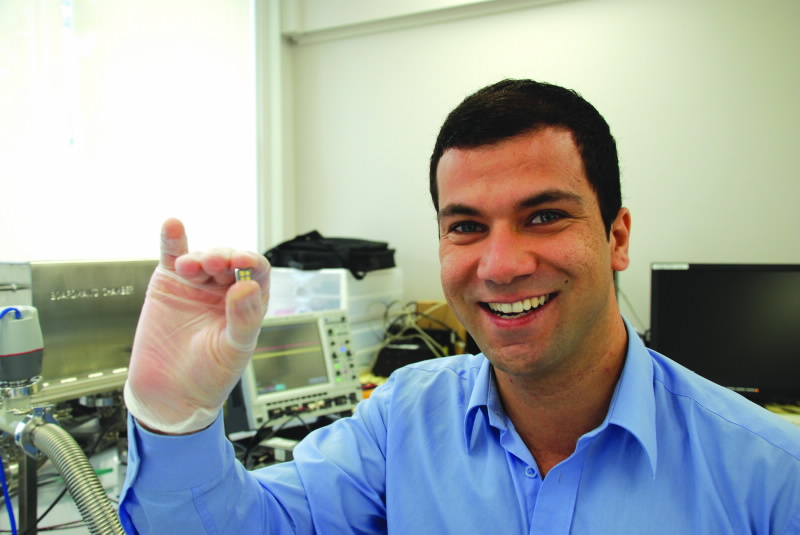 |
| Fig 2. Ramin Rafiei holding a 10 X 10 x 1.9 mm3 CdMnTe radiation detector. |
Compound semiconductors: CdMnTe a promising candidate
CdMnTe is a promising compound semiconductor. While previously investigated for applications in optical isolators (transmission of light in only one direction using the Faraday effect), infra-red detectors and tuneable solid state lasers, its application as a radiation detector was first investigated in 1999. [1]
Its distinct advantages of good compositional homogeneity and a highly tuneable band-gap (energy difference between the top of the valence band and the bottom of the conduction band in insulators and semiconductors) compared to CdZnTe and CdTe, which have been leading room temperature detector candidates for over three decades, have encouraged CdMnTe detector developments in recent years.
A detailed understanding of the fundamental charge transport properties of CdMnTe radiation detectors isessential for detector developments. The most useful figure of merit is the mobility-lifetime product which quantifies the charge carrier transport through the detector. While for silicon and germanium this figure is greater than unity, for compound semiconductors this figure is up to 100,000 times less.
The main cause of this performance shortfall can be traced to trapping centres caused by impurities and lack of stoichiometry in the material. Low mobility-lifetime product results in short carrier drift lengths and limits the maximum detector thickness and hence its application. It is also imperative to measure the uniformity of the charge transport properties across the detector, allowing for the identification of surface and bulk features which affect charge transport through the device.
ANSTO and Brookhaven National Laboratory jointly investigate and improve the performance of CdMnTe detectors [2] and their properties. The CdMnTe crystals were grown by the vertical Bridgman technique [2]. A manganese fraction of 5 %, corresponding to a band-gap of 1.59 eV, was chosen for optimum room temperature spectral performance.
To grow highresistivity CdMnTe, the crystal was doped with indium. Indium, which is a donor compensates for the high concentration of Cd vacancies which act as acceptor centres in CdMnTe.
The samples were cut to a size of 10 x 10 x 1.9 mm3. Infrared imaging of the CdMnTe samples prior to their clean-room fabrication revealed networks of tellurium inclusions distributed throughout their bulk, as shown in Fig. 1, and at an average concentration of 4.6 x 105 cm-3.
Clean-room CdMnTe detector fabrication
Each sample was mechanically polished with adeionised water-based slurry of alumina powder in order of decreasing alumina particle sizes of 1 μm, 0.3 μm and 0.05 μm until extremely smooth surfaces were achieved.
To prepare the CdMnTe crystal surfaces for metal contact deposition, each sample was etched in an optimum 0.1% bromine-methanol solution for 5 minutes. Prior to metal deposition, the four contacts on the front surface of the sample were patterned by photolithography.
To ensure excellent adhesion strength of the gold to the CdMnTe surface, we adopted a twostep thermal deposition of 5 nm chromium followed by a 150 nm gold layer. The detector test structures consist of a 2 x 2 array of evenly spaced 4 mm2 squares and π mm2 circles, both with and without guard rings. A single uniform contact covers the entire rear side. A fabricated CdMnTe detector is shown in Fig. 2.
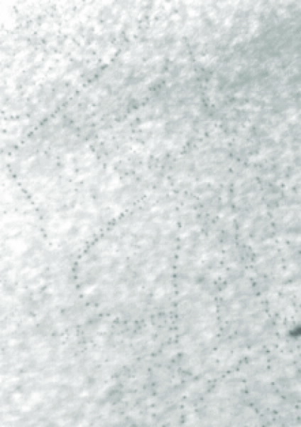 |
| Fig 1. An infrared image of a 1.2 X 2.0 mm2 area just beneath the CdMnTe surface. The dark dots are rellurium inclusions. The imag shows a network of tellurium which extend from one side of the crystal to the other. |
Charge-transport properties of CdMnTe
Time-resolved transient current measurements and alpha-spectroscopy measurements have been used to measure the charge-collection efficiency of CdMnTe detectors. Fig. 3 shows the dependence of the chargecollection efficiency on the applied bias voltage.
The average charge-collection efficiency across the detector increases with higher bias values and approaches 100% at the highest applied bias of 1000 V. The fit to the data points follows the Hecht analysis [3] and produces an average electron mobility-lifetime product of 8.5(±0.4) x 10-4 cm2V-1.
Uniform charge-carrier transport is critical to the spectroscopic performance of CdMnTe detectors. Ion beam induced charge (IBIC) measurements, utilising 4He2+ beams from the ANTARES accelerator at ANSTO, have revealed the charge transport of these devices down to micron scale resolution. Fig. 4 (top panel) is an IBIC image showing the charge collection efficiency across an area of 1449 x 1449 μm2 and at an applied bias of 400 V.
Such images have quantified how major impurities such as tellurium inclusions present within the detector bulk (and clearly visible in Fig. 4 as areas of reduced charge collection), affect the charge collection of these devices. These measurements have also shown that the role of tellurium inclusions in degrading charge collection is reduced with increasing values of bias voltage.
In contrast to the top panel of Fig. 4, the bottom panel is an IBIC image showing uniform charge collection at a value approaching 100%. The edges of the contact and the guard ring structure are clearly visible.
Single charge-transient measurements provided the drift time of the electrons across the detector. Using these transit times the drift velocity of the electrons has been calculated and is shown in Fig. 5, as a function of the applied electric field. From the region of proportionality in Fig. 5, the room temperature mobility of the CdMnTe sample was found to be 718(±55) cm2/Vs. Knowing the electron mobility-lifetime product the electron carrier lifetime is 1.2(±0.1) μs.
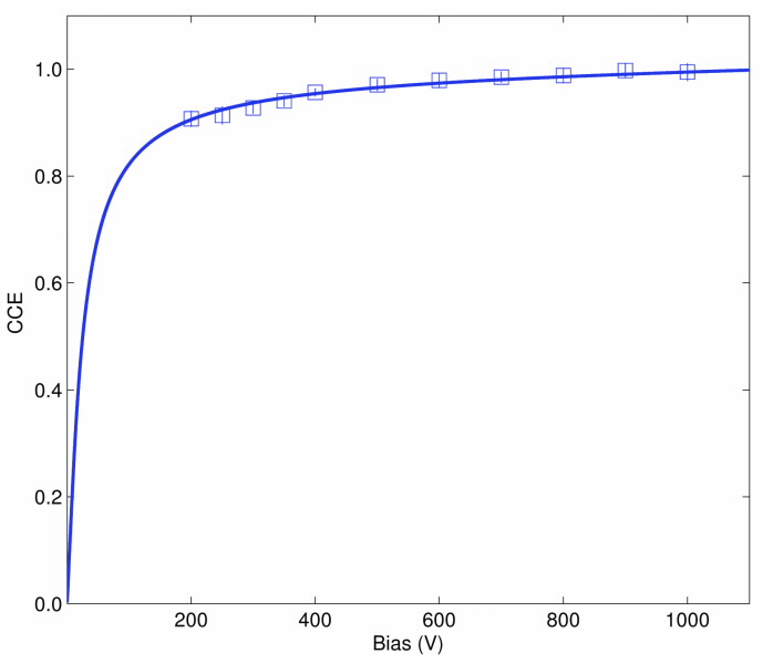 |
| Fig 3. The evolution of the average charge-colelction efficiency across the CdMnTe detector with applied bias voltage. The efficiency approaches 100% for e highest bias measurement. The measured data poins have been fitted usingthe Hecht model to obtain the mobility- lifetime product. |
Summary and Path Ahead
The ANSTO-Brookhaven detector collaboration covers the areas of crystal growth, detector fabrication and characterisation. Knowledge gained from our recent measurements has already led to the growth of CdMnTe crystals with modified stoichiometry.
These crystals have been fabricated into radiation detectors and initial measurements on these generation II devices show an order of magnitude improvement in the electron mobility-lifetime product. Continued improvements in crystal quality and detector fabrication will be required for the realisation of state-of-the-art radiation detectors in medical and national security applications.
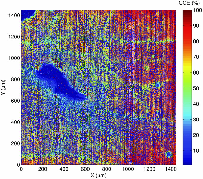 | 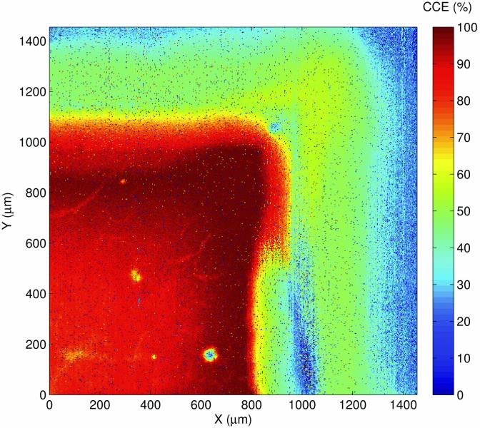 |
Fig 4. Spatially resolved charge-collection efficiency maps of the CdMnTe detector. On this colour scale blue signifies low charge collection, while regions of high charge collection are represented in red. In the top panel regions of poor efficiency are spread throughout the bul and are associated with the tellurium network. In contrast, a region with uniform charge collection approaching 100% is presented in the bottom panel. The edges of the contact and the guard ring structure (green coloured) are clearly visible. |
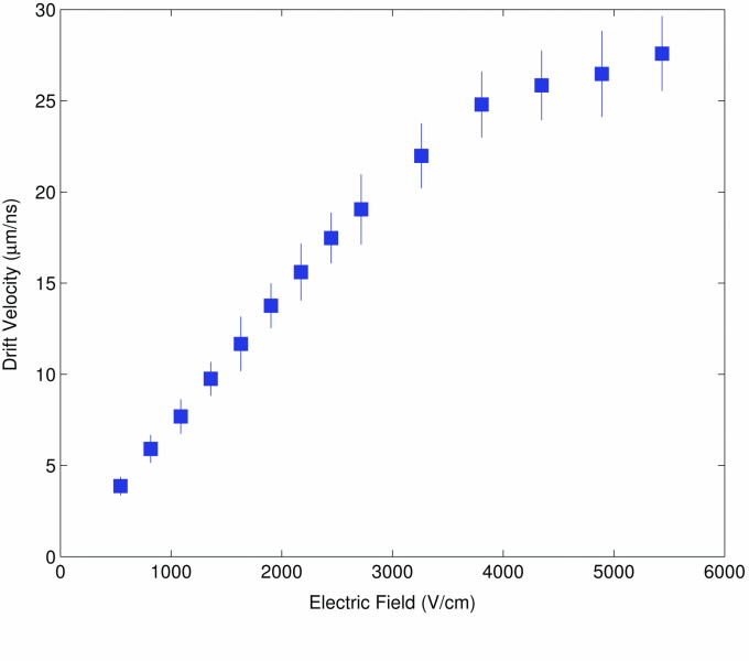 |
Fig 5. Carrier-drift velocity as a function of the applied electric field. From the region of proportionality the carrier mobilty has been extracted.
|
Authors
Aleksey E. Bolotnikov2, Ralph B. James2
1ANSTO, 2Brookhaven National Laboratory, USA
References
- A. Burger et al., Crystal growth, fabrication and evaluation of cadmium manganese telluride gamma ray detectors, J. Cryst. Growth, 198/199, 872-876 (1999).
- R. Rafiei et al., Investigation of the charge collection efficiency of CdMnTe radiation detectors, IEEE Trans. Nucl. Sci., 59, 634-641 (2012).
- Y. Nemirovsky, A. Ruzin, G. Asa, and J. Gorelik, Study of the charge collection efficiency of CdZnTe radiation detectors, J. Electron. Mater, 25, 1221-1231 (1996).
Published: 11/09/2012