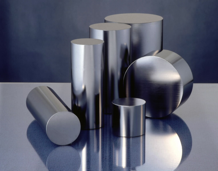
ANSTO is one of the worlds five big players in the silicon irradiation business, with its HIFAR nuclear research reactor producing high quality, high conductivity silicon for the computer industry.
 |
| HIFAR produces high quality, high conductivity silicon for the computer industry. |
Of the many organisations involved in the silicon irradiation business worldwide, ANSTO is one of the five big players with a 15% market share.
France, Denmark, Sweden and the United States make up the other four, but ANSTO is one of the favoured suppliers, because of its reactor capabilities, according to ANSTOs Robert Godfrey, who has managed its irradiation business for several years.
"Its all based on the QCD (Quality, Cost and Delivery) principle and we meet customer expectations in all those areas," he said.
Silicon irradiation, or Neutron Transmutation Doping (NTD), changes the properties of silicon, making it highly conductive of electricity.
Large, single crystals of silicon grown in Japan and shaped into ingots, are air freighted to ANSTO where they are prepared for irradiation inside the HIFAR reactor. Irradiation involves bombarding the ingots with neutrons for precise periods. One in each billion silicon atoms in each ingot is changed to phosphorous. This increases the efficiency of the silicon in conducting electricity, an essential characteristic for the electronics industry, though only about 5% of silicon is drawn from NTD.
"While irradiation is essential for some applications, such as high power discrete devices, transistors and memory chips, most other applications do not need such high quality," Mr Godfrey said.
"Therefore, the market for silicon irradiation is not huge, but it is significant financially. The money ANSTO earns from irradiation helps offset the operational costs of the reactor," he said.
NTD occurs after silicon ingots have been lowered into the reactors graphite reflector facilities, just outside its heavy water tank. Depending on the size of the ingot (they vary from 77mm in diameter to 200mm) and the electrical properties required by the client, irradiation can take anywhere from two hours to five days.
The silicon irradiated in HIFAR is returned to ANSTOs five Japanese clients- Shin Etsu, Mitsubishi Materials Silicon Corporation, Komatsu Electronic Metals, Toshiba Ceramics and, more recently, Sumitomo Sitix Corporation.
The amount of work generated for HIFAR by these five clients is equal to irradiation of approximately one tonne of silicon each month or more than 800 batches per year. With the onset of a predicted market slump this year, the amount to be processed at ANSTO is expected to drop.
"The fall in demand, will, however, allow us time to make the necessary changes to increase capacity to capture the expected later increased demand- and market share," Mr Godfrey said.
"Feedback from all five client companies has been very positive. All were pleased with the quality of our product and of our service, so HIFAR continues to be one of the favoured reactors," he said.
HIFAR is particularly attractive to the Japanese because of its high ratio of thermal neutrons to fast neutrons when silicon irradiation takes place. When fission occurs, fast neutrons released can cause damage to crystals by dislodging silicon atoms from their regular position in the materials structure.
In HIFAR, the silicon ingots are irradiated outside the reactors core, which is surrounded by heavy water, minimising exposure to fast neutrons.
This is why heavy water research reactors, particularly ANSTO's HIFAR and Denmarks DR-3 reactor, are in high demand.
ANSTO also has an edge over the other major players in that HIFAR is the only reactor which can accommodate 200mm crystals. Though the majority of ingots irradiated in HIFAR are just 101mm in diameter (45%), future demand will be for larger diameters, which reduces the number of available reactors.
Published: 11/04/1997


