Organic light-emitting diodes (OLEDs) are extensively used in devices such as television and mobile phone screens, but their life-time depends significantly on the stability of the chemical layers that form these devices.
 |
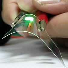
| Fig 1. A flexble OLED device (photo courtesy of Andrew Liszewski) |
Structural changes at the interfaces between these layers, which can occur during production or when the device heats up, dramatically affect how electrical charge travels through the device leading to changes in its performance.
ANSTO’s research used neutron reflectometry and specifically synthesised deuterated molecules that are typically used in OLEDs, to study the combining of layers and the structural changes that take place on the nanoscale, or sub-microscopic level, to improve the performance of the next generation of these devices.
What is an OLED?
Organic light-emitting diodes (OLEDs) are generally made of thin layers of organic or organometallic (macro) molecules sandwiched between two electrodes (Fig.1). The devices emit light when an electric current flows through them.
OLEDs are under intense investigation for use in the next generation of display and lighting technologies. These devices are used already in television screens, computer monitors and small portable system screens such as mobile phones and personal digital assistants.
How does an OLED work?
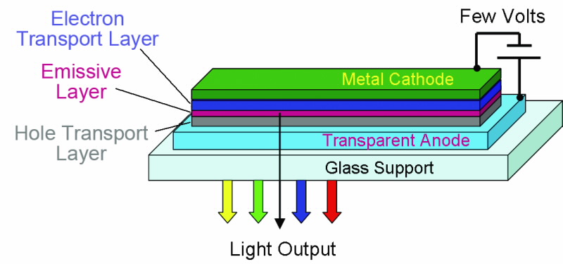
The simplest OLED has the emissive layer sandwiched between two electrodes (anode and cathode), one of which must be transparent to let the light escape. The anode injects holes into the device while the cathode injects electrons. When an appropriate voltage (typically a few volts) is applied to the cell the injected positive and negative charges recombine in the emissive layer to produce light (electroluminescence).
However, for the devices to work well there needs to be balanced injection and charge transport of holes and electrons and to do this, additional charge transport layers are often introduced between the electrodes and the emissive layer. Fig. 2 shows a typical device that contains an ‘electron transport layer’ and a ‘hole transport layer’ in addition to the light-emitting layer.
Scope of study
While efficiencies of OLEDs have risen quickly the task of preparing such devices with lifetimes suitable for displays and lighting has proved challenging. The morphological stability of the layers in the device can affect both device efficiency and lifetime.
Heat generated during operation is one of the critical factors which can contribute to the instability of the layers at the molecular interfaces.
This is particularly important for OLEDs based on small molecule phosphorescent iridium(III) complexes such as fac-tris(2-phenylpyridyl)iridium(III) [Ir(ppy)3] due to the different thermal properties of the materials in the adjacent layers, and also due to the fact that the complex is blended into a host material [e.g., 4,4-bis(N-carbazolyl)biphenyl = ‘CBP’].
In blends, it is difficult to elucidate whether the guest is evenly distributed throughout the film or whether there are concentration variations in parts of the film.
Investigations of functioning devices with buried interfaces present numerous difficulties using conventional surface-science techniques and so neutron reflectometry along with deuteration of specific molecular layers has become the key method for the study of the morphology, diffusion and interfacial behaviour in organic thin-film semiconducting devices.
These phenomena and the performance of organic optoelectronic devices are the subject of ongoing investigations by Paul Burn, Ian Gentle and their co-workers at the University of Queensland.
They have developed a combined in situ neutron reflectometry/ photoluminescence measurement that allows the simultaneous collection of the neutron reflectivity data and emission spectra from functioning OLEDs [1].
An additional feature of the experiment is that the sample can be heated in situ thus enabling the direct determination of the effect of annealing on the physical and photophysical properties.
 |
| Fig 2. Schematic of an OLED device. |
Why use neutrons and deuteration?
Neutron reflectometry is an excellent method for investigating the internal structure of thin (typically < 100 nm) films. In blended films, where there may be out-of-plane phase separation of the components within the blend, careful deuteration enables differentiation of components and allows any separation to be observed.
Deuteration is the process where all or part of the hydrogen (1H) content of a molecule is replaced by the stable (non-radioactive) isotope deuterium (2H = D).
Materials containing hydrogen (1H) are said to be protonated whilst those containing deuterium (2H = D) are said to be deuterated. The properties of the hydrogen and deuterium nuclei mean they scatter neutrons quite differently.
This difference manifests as a variation in a quantity called the neutron scatteringlength density.
Neutron-beam studies exploit thi difference in scattering-length density to probe the structures of individual components in multicomponent systems. In multi-layer films, a combination of deuterated and protonated layers can give excellent contrast in a neutron reflectometry experiment.
Deuteration of the OLED components
The National Deuteration Facility at ANSTO has the capability and expertise to deuterate a variety of (macro) molecules: this includes biodeuteration of proteins and polymers, as well as chemical deuteration including the synthesis and deuteration of a range of compounds such as surfactants, lipids, fatty acids, sugars and other small organic molecules.
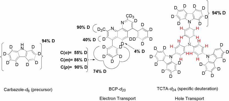
Conjugated aromatic heterocycles such as bathocuproine (BCP) and tris(4-carbazoyl-9-ylphenyl) amine (TCTA) (Fig. 3) are widely used in OLEDs as electron and hole transport materials respectively.
Deuteration of these aromatic and heterocyclic molecules enables the characterisation of the film structure typically found in multilayer OLEDs, due to a substantial increase in neutron scattering-length density of the deuterated material compared to their equivalent protonated forms.
In addition, we can probe interdiffusion between the different molecular layers under thermal stress [1-3].
A combination of spectroscopic techniques such as nuclear magnetic resonance (NMR) and mass spectroscopy (MS) were used to calculate the total deuterium content in the molecules and the relative occurrence of hydrogen and deuterium atoms at specific sites within the molecule.
NMR is a particularly useful analytical tool as experiments can be designed that discriminate between resonances of the various types of carbon molecules present: fully deuterated groups (CD, CD2, CD3), partially deuterated groups (CHD, CHD2, CH2D), and non-deuterated groups (C, CH, CH2, CH), thus allowing the full characterisation of the deuterated molecules, and hence the calculation of the scatteringlength density of the different materials in the OLED layers for the neutron experiments [3].
 |
| Fig 3. Deuerated molecules used in this study. |
Hydrothermal deuterium labelling
Deuteration of the molecules for this work was achieved either by H/D exchange reactions with deuterium oxide (D2O) catalysed by Pt/C and Pd/C under hydrothermal conditions, or by synthesis from deuterated precursors produced by the same method.
Hydrothermal deuteration involves heating the protonated version of the molecule in D2O, which acts as the solvent and deuterium source, in the presence of metal catalysts under high temperatures and pressures using a Parr reactor (see image p.58).
These reactors are designed to heat aqueous solutions to temperatures approaching water’s supercritical temperature under pressure.
This induces H/D exchange between sites on the protonated molecule to produce a deuterated version which is then isolated, purified and characterised.
Inter-diffusion and phase separation in OLEDs
Thin films of the desired protonated and deuterated compounds were prepared by thermal evaporation under high vacuum onto silicon wafers at the University of Queensland for neutron reflectivity measurements on the Platypus time-of-flight neutron reflectometer at the OPAL 20 MW research reactor at ANSTO [4].
 |
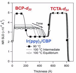
| Fig 4. Neutron scattering-length density profile from an OLED trilayer from neutron reflectivity data showing interdiffusion of BCP-d20 and Ir |
Analysis of neutron reflectivity data from a BCP-d20 / (Ir(ppy)3:CBP) / TCTA-d24 trilayer film on silicon (Si) measured at room temperature gave thicknesses of 15 nm, 35 nm and 27 nm respectively with excellent contrast between the BCP-d20 and TCTA-d24 layers (SLD~5x10⁻⁶ Å-2) and the (Ir(ppy)3:CBP) layer (SLD~2.5x10⁻⁶ Å-2).
The three-layer structure was stable at temperatures up to 90°C. At 100°C the Ir(ppy)3:CBP and BCP-d20 layers were found to interdiffuse, while the (TCTA-d24) / Ir(ppy)3:CBP interface remained stable (Fig. 4).
Only by using deuterated BCP-d20 and TCTA-d24 could we study this behaviour as the protonated forms of BCP and TCTA in these thin-film devices would not have provided adequate scattering contrast between the CBP emissive layer, the BCP and the TCTA layer.
In addition, our study found that as prepared blended films of Ir(ppy)3 in CBP were uniformly mixed. However the stability of the films with respect to phase separation was strongly dependent on the weight ratio of the Ir(ppy)3 in CBP.
When films comprised of 6 wt% Ir(ppy)3 in CBP (typically used in OLEDs) were heated to a moderate temperature (at 80°C) they were found to phase separate. In contrast, simply increasing the weight percent to 12wt% caused the film to become stable such that on heating no significant separation occurred.
These results have important implications for materials and device design, not only for OLEDs but also for stacked organic photovoltaic devices.
It is important to identify the temperature at which these devices can work reproducibly and most efficiently, as well as the environment in which these devices are being used or stored.
Authors
Tamim A. Darwish1 Michael James1, Peter J. Holden1, Arthur R. G. Smith,2 Ian R. Gentle2, Paul L. Burn2.
1ANSTO, 2University of Queensland
References
- Smith, A. R. G., Ruggles, J. L., Cavaye, H., Shaw, P., Darwish, T. A., James, M., Gentle, I. R., Burn, P. L., Morphology and Stability of Fac-tris(2-phenylpyridyl) iridium(III) Blended Films: a Neutron Reflectometry Study, Advanced Functional Materials, 21(12), 2225-2231 (2011).
- Smith, A. R. G., Lee, K. H., Nelson, A., James, M., Burn, P. L., and Gentle, I. R., Diffusion – the Hidden Menace in Organic Optoelectronic Devices, Advanced Materials, 24(6), 822-826 (2012).
- Darwish, T. A., Smith, A. R. G., Gentle, I. R., Burn, P. L., Luks, E., Moraes, G., Gillon, M., Holden, P. J., and James, M, Deuteration of conjugated aromatic heterocycles for morphological studies of organic light emitting devices, Tetrahedron Letters, 53, 931–935 (2012).
- James, M, Nelson, A, Holt, SA, Saerbeck, T, Hamilton, WA and Klose, F, The multipurpose time-of-flight neutron reflectometer “Platypus” at Australia’s OPAL reactor, Nucl. Instrum. Methods Phys. Res., Sect. A 632(1), 112-123 (2011).
Published: 19/07/2012


